Nanomechanics of graphene and 2-dimensional (2D) materials
Due to sp2 bond of carbon atoms in graphitic carbon materials, their stiffness and strength have been expected to be very high. We have characterized single layer graphene’s elastic properties and strength by using the AFM indentation technique. It’s Young’s modulus has been measured to be 1TPa (close to that of diamond) and its fracture strength 130GPa, which is about 200 times higher than standard steel. We are characterizing mechanical properties of multi-layer and hydrogenated graphene, and other 2-dimensional nanomaterials. The goal of this research is to observe the characteristics of the atomic bonds and to establish new theories on 2D materials’ mechanical behavior at nanoscale.
(reference: Science, vol 321, p385, 2008,)

Nanotribology of graphene and 2-dimensional materials
Graphene’s mother material, graphite, has been widely known as an excellent lubricant because of easy slippery between the layers. We characterized the frictional characteristics of graphene and 2D materials using an AFM friction measurement technique and found that atomically thin graphene and 2D materials has higher friction than their thicker counterparts. We found out that when an AFM tip scans over it, it bends and bulges up and the friction increases due to “puckering effect”. Since 2D nanomaterials are expected to be used as coatings for lubrication, this finding will enable us to control friction between the thin coatings and contact surface.
(reference: Science, vol 328, p76, 2010)

Electrical properties of hexagonal boron nitride (h-BN)
As graphene, h-BN has a hexagonal lattice structure and excellent mechanical and thermal properties. However, electrically it is an insulator unlike graphene. Our study showed that h-BN is an ideal gate-insulator for graphene due to its ultra-flatness as a 2D material. We are planning to synthesize large area h-BN films to use an insulator for graphene electronics and to make h-BN composites with high thermal conductivity, low electrical conductivity and high optical transmittance.
(reference: Nature nanotechnology, vol 5, p722, 2010)
Electrical and optical properties of molybdenum disulfide (MoS2)
MoS2 is another 2D material and a semiconductor. Interestingly, our study revealed its electronic bandgap changes with thickness (or number of layers). Also single layer MoS2 has a direct bandgap unlike bi- and thicker layers. The bandgap modulation with thickness is quite a unique phenomenon and needs to be investigated further. This phenomenon can be applied to the development of optical sensors, light emitters, and lasers.
(reference: ACS nano, vol 4, p2695, 2010 & physical review letters, vol 105, p136805, 2010)

Electrical and optical properties of molybdenum disulfide (MoS2)
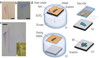
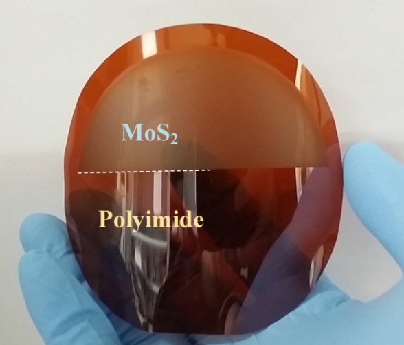
For the future application of 2D semiconductors for flexible electronics and wearable electronics, 2D metal chalcogenides should be synthesized at large sizes as the continuous film forms. We have been synthesizing MoS2 thin films from monolayer on wafers such as SiO2/Si, quartz, sapphire using thermal chemical vapor deposition methods. Also we have synthesized MoS2 directly on a plastic substrate (polyimide) by the plasma enhanced chemical vapor deposition (PECVD).
(reference: Nanoscale, 6, 2821, 2014; Advanced Materials, 27, 5223, 2015)

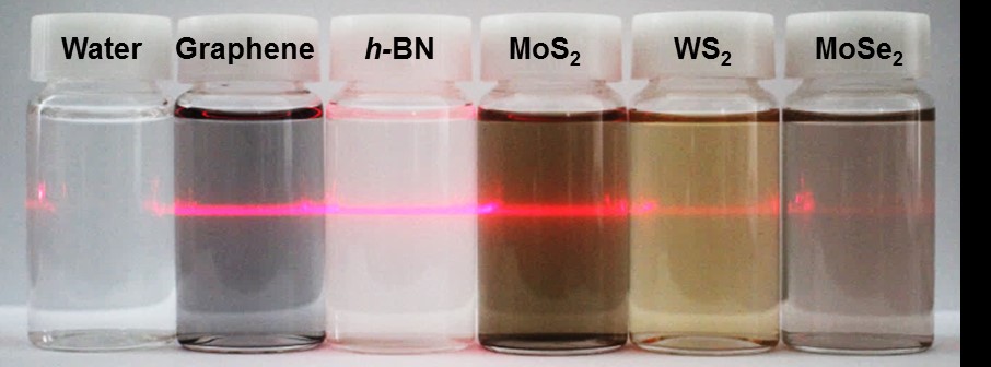
Dispersion of 2D materials in water
Graphene and 2D materials are usually not dissolved in water due to the hydrophobic properties of these materials. However, we have developed a new technique to disperse 2D materials in pure water without using any chemicals or surfactants. By elevating the temperature while exfoliating bulk materials, some materials are functionalized by cavitation effect and some exhibits polarity of their own.
(reference: Nature comm., DOI: 10: 1038/ncommns9292,2015)